Solder Resist for Package Substrates (SR Series)

Material for PWBs

Overview

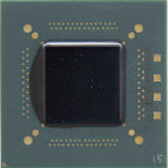
Resonac’s photosensitive solder resist materials protect and insulate high-density wiring used for semiconductor packages.
Resonac boasts a large market share in the field of semiconductor packages using flip-chip packaging.

Features

  • Realizes low warpage due to low CTE and low shrinkage.
  • Contributes to higher density semiconductor packages due to high resolution.
  • Contributes to high reliability (TCT and reflow resistance, etc.) due to high heat resistance.
  • Offers the liquid type SR7300 and film type SR-F series.

Product Characteristics & Line-Up

Available upon request for film thickness

Thermal Cycle Test

TEST Vehicle

CSAM:Constant-depth mode Scanning Acoustic Microscope

Contact Us

General Enquiry

Opening hours:
9:00 a.m.~5:00 p.m.
(Monday to Friday)

    Product Enquiry

    <h3>I have read the <a href='/privacy-policy' target='_blank'>privacy policy</a> and agree</h3> Lorem ipsum dolor sit amet, consectetur adipiscing elit. Etiam eu turpis molestie, dictum est a, mattis tellus. Sed dignissim, metus nec fringilla accumsan, risus sem sollicitudin lacus, ut interdum tellus elit sed risus.

    Film for Circuit Formation in Direct Imaging (RD Series)

    Photosensitive Film (Photec)

    Overview

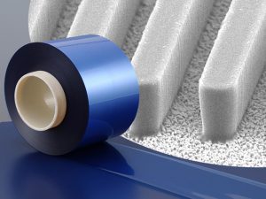
    Resonac’s resist materials for forming printed wiring board circuits are applicable to direct-writing exposure machines that pattern circuits using laser beams.

    Features

    • Provides excellent shaped resist profiles, and is capable of forming fine-pitch circuits based on film thickness.
    • Responds to circuit formation by semi-additive processing.
    • Applicable to direct-writing exposure machines.

    Film Characteristics & Line-Up

    ※DE-1 UH was applied(Adtec Engineering Co.,Ltd, 405 nmDI)
    Substrate roughness Ra:0.4 µm
    Post exposure bake (P.E.B) : 80 degree C, 30 Sec. (Box Oven)
    Developer : 1.0 wt% Na2CO3aq., 30 degree C, 0.16 MPa

    Resist Profile

    Contact Us

    General Enquiry

    Opening hours:
    9:00 a.m.~5:00 p.m.
    (Monday to Friday)

      Product Enquiry

      <h3>I have read the <a href='/privacy-policy' target='_blank'>privacy policy</a> and agree</h3> Lorem ipsum dolor sit amet, consectetur adipiscing elit. Etiam eu turpis molestie, dictum est a, mattis tellus. Sed dignissim, metus nec fringilla accumsan, risus sem sollicitudin lacus, ut interdum tellus elit sed risus.

      Film for Package Substrate Circuit Formation (RY Series)

      Photosensitive Film (Photec)

      Overview

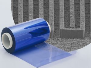
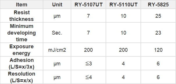
      Resonac’s photosensitive resist materials designed to form fine-pitch circuits on semiconductor package substrates can form circuits with a film thickness of 10 um or less and a width of 4 um or less.

      Features

      • Provides excellent shaped resist profiles, and is capable of forming fine-pitch circuits based on film thickness.
      • Responds to circuit formation by semi-additive processing.
      • Responds to resist patterning using a stepper exposure machine.

      Film Characteristics & Line-Up

      Projector machine; i-line projector
      Developing conditions; 1.0 wt% Na2CO3aq, 30 ℃, Minimum developing time×2

      Resist Profile

      Contact Us

      General Enquiry

      Opening hours:
      9:00 a.m.~5:00 p.m.
      (Monday to Friday)

        Product Enquiry

        <h3>I have read the <a href='/privacy-policy' target='_blank'>privacy policy</a> and agree</h3> Lorem ipsum dolor sit amet, consectetur adipiscing elit. Etiam eu turpis molestie, dictum est a, mattis tellus. Sed dignissim, metus nec fringilla accumsan, risus sem sollicitudin lacus, ut interdum tellus elit sed risus.

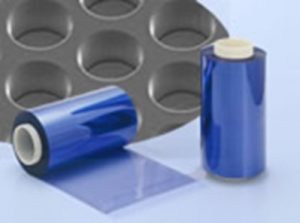
        Film for Thick Film Resist Formation (HM Series)

        Photosensitive Film (Photec)

        Overview

        Resonac’s photosensitive materials designed to form thick resist pattern layers are used for such applications as the copper plating process of printed wiring boards requiring a high aspect ratio and electroforming in metal mask manufacturing.

        Features

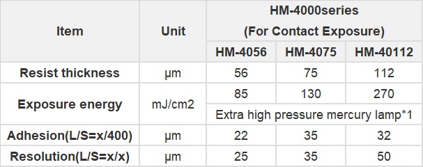
        • Superior resolution/adhesion and is capable of forming resists with a thickness more than double the hole diameter and line width.
        • Offers a thick film lineup (35-168 um) in response to various applications.
        • Superior chemical resistance, and applicable as a resist for copper plating and electroplating.
        • Responds to development with standard sodium carbonate solutions and peeling solutions used for printed wiring boards.
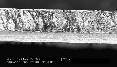
        • Provides smooth sidewall shapes.

        Film Characteristics & Line-Up

        ※1Collimated light type

        Resist Profile

        Contact Us

        General Enquiry

        Opening hours:
        9:00 a.m.~5:00 p.m.
        (Monday to Friday)

          Product Enquiry

          <h3>I have read the <a href='/privacy-policy' target='_blank'>privacy policy</a> and agree</h3> Lorem ipsum dolor sit amet, consectetur adipiscing elit. Etiam eu turpis molestie, dictum est a, mattis tellus. Sed dignissim, metus nec fringilla accumsan, risus sem sollicitudin lacus, ut interdum tellus elit sed risus.

          Thermal Conductive Sheets (TC)

          Semiconductor (Backend)

          Overview

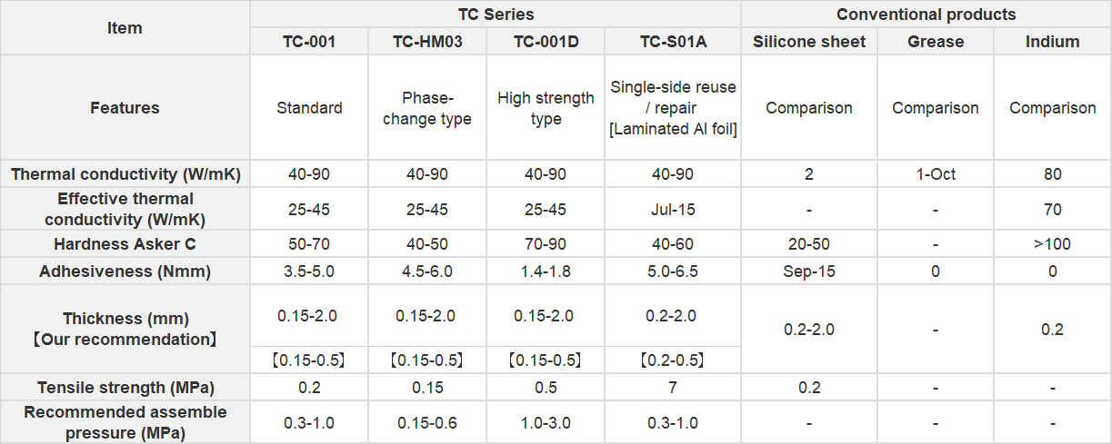
          Resonac’s thermal conductive sheets (TIM material) with electrical conductivity efficiently release heat from IC chips when applied a semiconductor package, and between IC chip and a heat spreader, heatsink or heat pipe.

          Features

          • Achieves high thermal conductivity in the thickness direction by vertically aligned graphite fillers.
          • Increases thermal conductivity by flexibly filling in gaps caused by differences in chip heights or uneven adhesive interface.
          • Possible to temporarily fix on heat modules with slight adhesiveness.
          • Applicable to next-generation large devices by flexibly fitting warped substrates.

          Sheet Characteristics & Line-Up

          Example

          Expected field of application

          The product’s superior thermal conductivity and cooling effect are expected to contribute to enhancing electronic device reliability and energy efficiency.

          Contact Us

          General Enquiry

          Opening hours:
          9:00 a.m.~5:00 p.m.
          (Monday to Friday)

            Product Enquiry

            <h3>I have read the <a href='/privacy-policy' target='_blank'>privacy policy</a> and agree</h3> Lorem ipsum dolor sit amet, consectetur adipiscing elit. Etiam eu turpis molestie, dictum est a, mattis tellus. Sed dignissim, metus nec fringilla accumsan, risus sem sollicitudin lacus, ut interdum tellus elit sed risus.

            Sintered Copper Paste

            Die Bonding Paste (DBP)

            Overview

            Highly efficient SiC (silicon carbide) power modules are becoming increasingly popular in electric vehicles (xEVs) for extending cruising range and improving fuel and electricity consumptions. A power module is composed of multiple power semiconductor chips mounted on a substrate in a package and a cooler bonded to a package. In addition to its high efficiency, SiC can be operated at high junction temperatures, enabling power modules with a higher output in smaller sizes. Making the most of SiC’s advantage, components of power modules, including die-bonding and bonding materials, are required to offer high heat resistance, heat dissipation and reliability.

            Currently, bonding with sintered silver paste (hereinafter, “sintered silver”), instead of conventional high-lead solder, is applied to SiC die-bonding. Although its heat resistance and dissipation properties, there is a concern of its reliability to achieve the further smaller, and higher output modules.

            Resonac proposes sintered copper paste (hereinafter, “sintered copper”) as a bonding material with superior heat resistance, heat dissipation, and reliability. Bonding with sintered copper enhances the reliability of SiC power modules while maintaining the same level of heat dissipation as sintered silver. Resonac has also developed sintered copper paste for large-area use, which is suitable for bonding between packages and coolers.

            Innovative Solution

            • Enhancing module reliability by bonding with sintered copper, featured by a higher hardness and lower CTE than silver

            Fatigue caused by the stress and strain tends to be accumulated in the die-bonding part with sintered silver, because silver, its main component, is soft and easily deformable. At power cycle tests, the repeated ON/OFF leads to stress accumulation in the die-bonding part and may result in fatigue destruction because of the differences in the coefficient of thermal expansion (CTE) among semiconductor chips, insulating substrates and die-bonding materials. On the other hand, copper is known for its higher elasticity and yield stress, lower CTE than silver. Bonding with sintered copper, Resonac offers, allows superior reliability because of less thermal strain than sintered silver and less probable to fatigue failures due to its thermal strain being contained within the elastic deformation.

            As bonding between packages and coolers, low thermal conductivity of conventional high-lead solder leads to a bottleneck in heat dissipation, while sintered silver remains a concern on reliability as more stress accumulation in the larger bonding area than the die-bonding part.

            To overcome these concerns, Resonac offers sintered copper paste optimized for large-area bonding. Resonac’s developing product allows thermal compression bonding at a lower pressure than the current sintered silver. Resonac’s sintered copper paste contributes to the higher output and smaller size of SiC power modules, with its superior reliability demonstrating the same level of thermal conductivity as sintered silver.

            Product Features

            • Superior reliability

            A power cycle test at T j ,max = 175℃ reveals that sintered copper has a characteristic life approximately 40 times higher than high-lead solder, and approximately five times higher than sintered silver.

            i. Power Cycle Test Weibull Analysis Results (Tj ,max = 175 ℃)
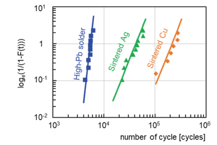
            The data shown are representative values that represent examples of the results of measurements, calculations, etc., and are not guaranteed values.

            • Heat dissipation equivalent to sintered silver

            Below are temperature distribution diagrams comparing samples using sintered copper and high-lead solder as die-bonding materials. Bonding with sintered copper, whose thermal conductivity of 300W/(m・K) is equivalent to sintered silver, allows to dissipate heat from SiC modules to periphery and prevents local temperature of rising. On the other hand, bonding with high-lead solder with a thermal conductivity of 30W/(m・K) leads to a bottleneck of heat dissipation in the die-bonding part.

            i. Temperature distribution on sample cross-sections
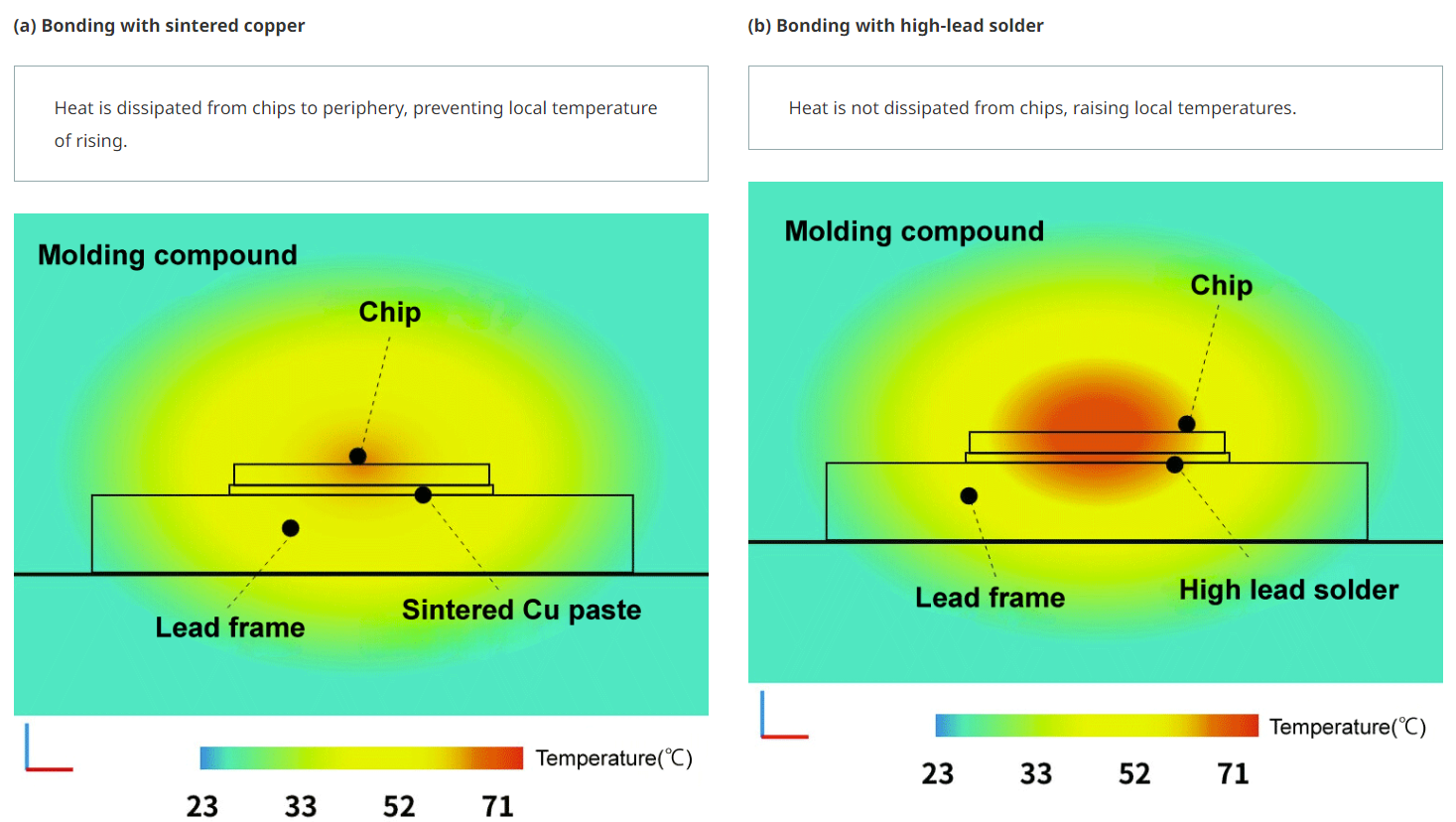
            (Items set other than material properties)
            Electrical power, environment temperature: measured values of samples, air properties: air at normal pressure and 30℃ (other physical quantities: fixed values), density: 1.161 kg/m3 , thermal conductivity: 2.610 x 10⁻² W/(m∙K), coefficient of molecular viscosity: 1.840 x 10⁻⁵ N∙s/m2 , thermal expansion coefficient: 3.333 x 10⁻³K -1 , conduction, radiation, heat transfer by natural convection, buoyancy, and turbulence were taken into account.

            The data shown are representative values that represent examples of the results of measurements, calculations, etc., and are not guaranteed values.

            • Developing two types of products for die-bonding and large-area bonding that contribute to heat dissipation design as modules
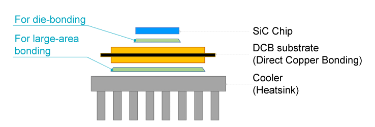
            Resonac offers two types of developing products for die-bonding and large-area bonding, whose paste components are optimized to each bonding part.; As for die-bonding use, 5 mm to 13 mm squares, as for large-area 30 mm to 50 mm squares. For large-area bonding use, especially, sintered copper allows fewer total loads of thermo-compression at a lower pressure, enabling superior reliability than sintered silver.
            Contact Us

            General Enquiry

            Opening hours:
            9:00 a.m.~5:00 p.m.
            (Monday to Friday)

              Product Enquiry

              <h3>I have read the <a href='/privacy-policy' target='_blank'>privacy policy</a> and agree</h3> Lorem ipsum dolor sit amet, consectetur adipiscing elit. Etiam eu turpis molestie, dictum est a, mattis tellus. Sed dignissim, metus nec fringilla accumsan, risus sem sollicitudin lacus, ut interdum tellus elit sed risus.

              N-CS Series

              Infocommunications

              Overview

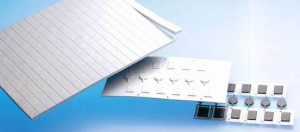
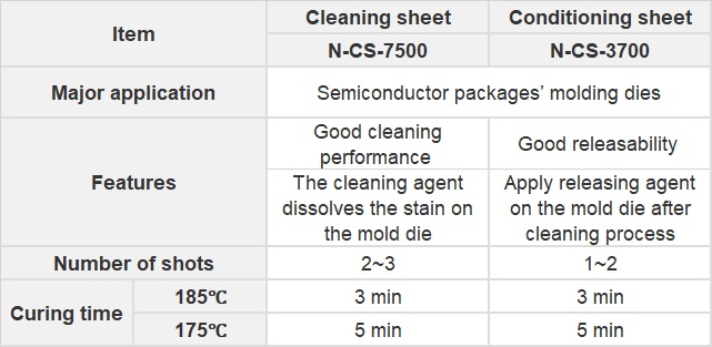
              Resonac’s Cleaning Sheet for encapsulation molding dies of semiconductor packages.
              By placing the sheet between dies and heating it, stains are transferred to the sheet and removed.

              How to Use

              Features

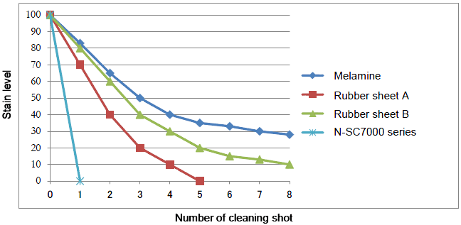
              • Remove stains with fewer shots than melamine cleaning materials, thereby reducing the cleaning time.
              • Remove stains in cavities, burrs on dies, and gas stains in air vents.
              • Environment-friendly cleaning agent prevents damage and corrosion of molding dies.

              Sheet Characteristics & Line-Up

              Cleaning Performance

              High filling type W Series

              With its original form and structure, W series completely fills cavity of mold die without air

              • W series is suitable for molding die with small cavity for small-sized semiconductor, diodes and mini transistor.
              • W seires is designed in a way that cavity is not blocked when the sheet is set on the mold die at any position.
              • With W series, the air inside cavity can completely escape to outside and can remove off stains from the entire cavity.

              Contact Us

              General Enquiry

              Opening hours:
              9:00 a.m.~5:00 p.m.
              (Monday to Friday)

                Product Enquiry

                <h3>I have read the <a href='/privacy-policy' target='_blank'>privacy policy</a> and agree</h3> Lorem ipsum dolor sit amet, consectetur adipiscing elit. Etiam eu turpis molestie, dictum est a, mattis tellus. Sed dignissim, metus nec fringilla accumsan, risus sem sollicitudin lacus, ut interdum tellus elit sed risus.

                EPINAL Series

                Die Bonding Paste (DBP)

                Overview

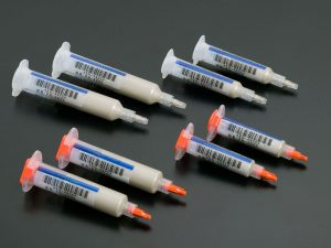
                Resonac’s solvent-free die bonding paste (conductive and non-conductive types) bonds chips to leadframes and organic substrates when manufacturing semiconductor packages.

                Resonac offers a wide-ranging lineup with its die bonding paste holding a large global market share.

                Features

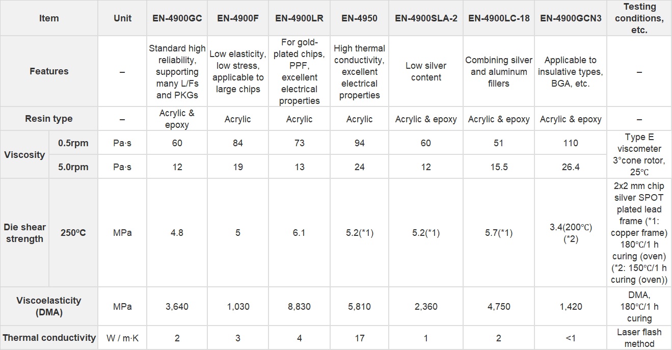
                • Low elastic modulus and high adhesive strength realizes greater reliability even for MSL1
                • Suitable for package on leadframes and organic substrates
                • Low-cost type using both aluminum and silver filler is also available
                • High thermal conductivity (17W/m-K) type effective for power devices and modules is lined up

                Paste Characteristics & Line-Up

                Contact Us

                General Enquiry

                Opening hours:
                9:00 a.m.~5:00 p.m.
                (Monday to Friday)

                  Product Enquiry

                  <h3>I have read the <a href='/privacy-policy' target='_blank'>privacy policy</a> and agree</h3> Lorem ipsum dolor sit amet, consectetur adipiscing elit. Etiam eu turpis molestie, dictum est a, mattis tellus. Sed dignissim, metus nec fringilla accumsan, risus sem sollicitudin lacus, ut interdum tellus elit sed risus.

                  Acrylonitrile

                  Automotive

                  Overview

                  Acrylonitrile is an organic compound used primarily in the production of plastics, but also in the production of fibers and synthetic rubber.

                  Our AN is an eco-friendly raw material certified by International Sustainability and Carbon Certified (ISCC). This certification proves that our products are produced using environmentally sustainable production processes and minimize carbon emissions.

                  Our products are produced by sustainable supply chains with minimal impact on the environment. We are actively working to build a more sustainable future, and ISCC certification is part of the effort. By choosing our products, you also play a part in a sustainable future. Please come and experience our products.

                  Sustainability and quality combined, that’s our promise.

                  Applications

                  • ABS resin for Plastic of Electronics, Automotives
                  • Carbon fiber for Airplane, Automotive Parts
                  • Adiponitrile for Nylon66 ABS

                  • Acrylic Fiber for Manmade fiber
                  • Nitrile Butadiene Rubber(NBR) for Synthetic Rubber in Automotive, Belt, Shoes.
                  • Acrylamide for Water treatment, Paper Additives

                  Packing Size

                  Bulk 1000MT~

                  Contact Us

                  General Enquiry

                  Opening hours:
                  9:00 a.m.~5:00 p.m.
                  (Monday to Friday)

                    Product Enquiry

                    <h3>I have read the <a href='/privacy-policy' target='_blank'>privacy policy</a> and agree</h3> Lorem ipsum dolor sit amet, consectetur adipiscing elit. Etiam eu turpis molestie, dictum est a, mattis tellus. Sed dignissim, metus nec fringilla accumsan, risus sem sollicitudin lacus, ut interdum tellus elit sed risus.

                    Die Attach Film (DAF)

                    Semiconductor (Backend)

                    Overview

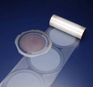
                    Resonac’s die attach films (DAF) combine function of dicing tapes and die bonding films suitable for semiconductor wafer singulation and bonding process.

                    Features

                    • Contributes to the reliability of semiconductor packages using DAF technology that provides low elasticity with excellent thermal stress relaxation, high adhesive strength, and superior heat resistance.
                    • Wide variety of products for applications from 3D NAND and DRAM memory devices to lead frames.
                      • Film thickness from ultra-thin types to thick types for FOW (film over wire) and FOD (film over die) applications.
                      • High Elastic modulus for good wire bondability of small chip
                      • Suitable for new processes such as SDBG (Stealth Dicing Before Grinding), in addition to conventional blade dicing.
                    • Excellent thermosetting adhesive film technology is used to expand various applications.
                      Offer DAF single layer products for electronic components and modules.

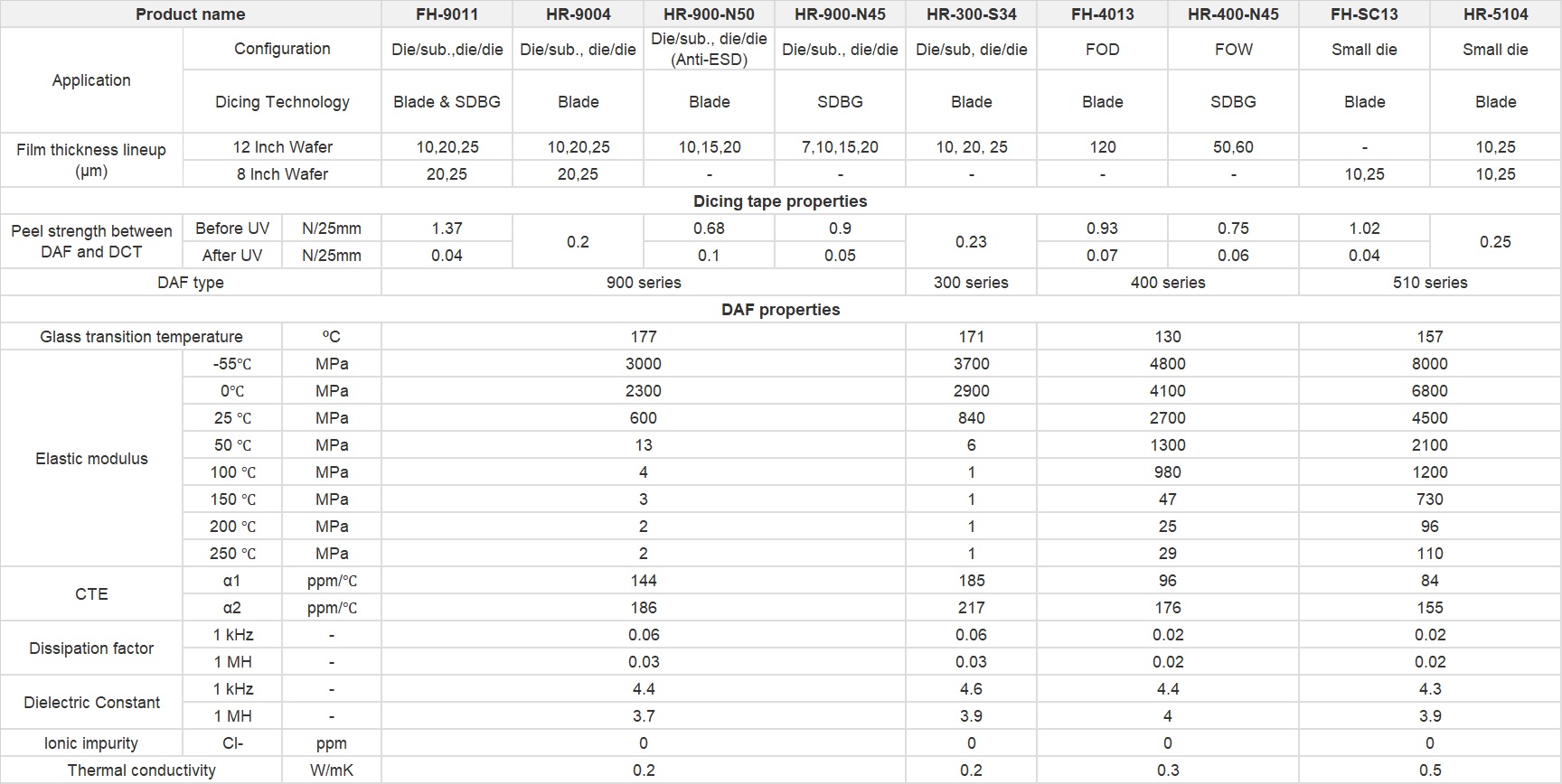
                    Film Characteristics & Line-Up

                    *The data in this table are representative values and do not guarantee quality. The values are subject to change without notice due to the optimization of measurement conditions or other reasons.

                    Contact Us

                    General Enquiry

                    Opening hours:
                    9:00 a.m.~5:00 p.m.
                    (Monday to Friday)

                      Product Enquiry

                      <h3>I have read the <a href='/privacy-policy' target='_blank'>privacy policy</a> and agree</h3> Lorem ipsum dolor sit amet, consectetur adipiscing elit. Etiam eu turpis molestie, dictum est a, mattis tellus. Sed dignissim, metus nec fringilla accumsan, risus sem sollicitudin lacus, ut interdum tellus elit sed risus.